Moments in Materials Seminar
Via Contact Tunneling Spectroscopy with Two-dimensional Materials
Presented by Evan Telford, Roy Group
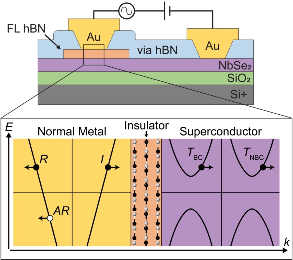
The study of two-dimensional (2D) materials is one of the fastest growing fields in condensed matter physics. These materials promise to revolutionize nanotechnology due to the ability to easily isolate clean atomically-thin sheets of conducting material for use in atomic-scale circuits1,2. Since the initial demonstration of the electric-field effect in devices fabricated from mechanically exfoliated graphene3, the number of available 2D compounds that can be integrated into nanocircuits has grown exponentially to encompass diverse electronic properties such as semiconductors, superconductors, and magnets. A significant engineering challenge within the 2D community concerns fabricating pristine interfaces between 2D materials with disparate electronic properties. Further complicating this problem is the observed air sensitivity of many 2D materials that manifest exotic correlated electronic phenomena. In this talk, I will introduce a platform for interfacing with air-sensitive 2D materials based on vertical interconnect access (via) contacts4 and discuss how we use this platform to examine tunnel junctions between a normal metal (Au) and a 2D superconductor (NbSe2) separated by an insulating tunnel barrier (few-layer hBN). This technique is extremely versatile, allowing us to explore how barrier height, barrier area, and barrier defect density affect the resulting tunneling spectra in both normal and superconducting states.
References:
(1) Novoselov, K. S.; Jiang, D.; Schedin, F.; Booth, T. J.; Khotkevich, V. V; Morozov, S. V; Geim, A. K. Two-Dimensional Atomic Crystals. Proc. Natl. Acad. Sci. U. S. A. 2005, 102 (30), 10451–10453.
(2) Novoselov, K. S.; Mishchenko, A.; Carvalho, A.; Neto, A. H. C. 2D Materials and van Der Waals Heterostructures. Science 2016, 353 (6298), aac9439.
(3) Novoselov, K. S.; Geim, A. K.; Morozov, S. V; Jiang, D.; Zhang, Y.; Dubonos, S. V; Grigorieva, I. V; Firsov, A. A. Electric Field Effect in Atomically Thin Carbon Films. Science 2004, 306 (5696), 666–669.
(4) Telford, E.; Benyamini, A.; Rhodes, D.; Wang, D.; Jung, Y.; Zangiabadi, A.; Watanabe, K.; Taniguchi, T.; Jia, S.; Barmak, K.; Pasupathy, A.; Dean, C. R.; Hone, J. C. Via Method for Lithography Free Contact and Preservation of 2D Materials. Nano Lett. 2018, acs.nanolett.7b05161.